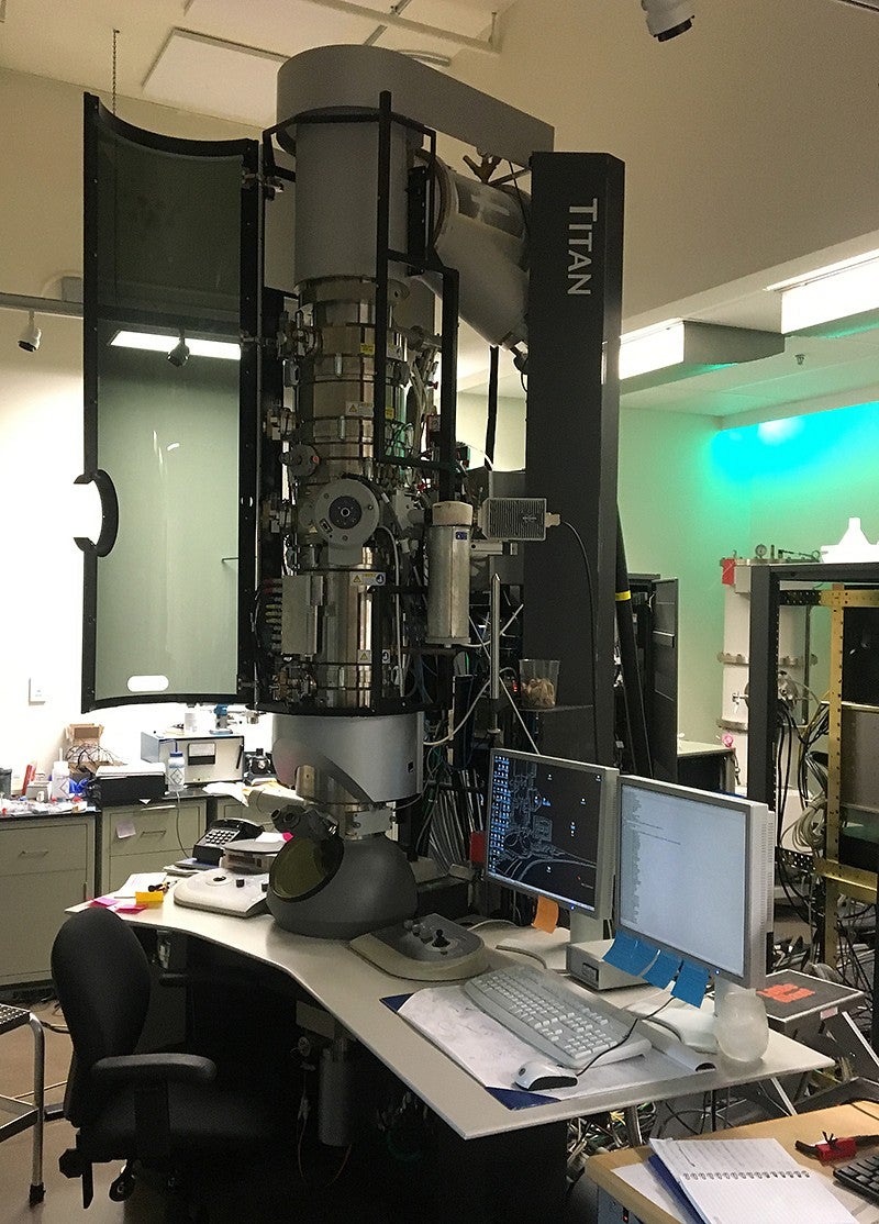
Researchers in Ben McMorran’s University of Oregon physics lab had a great 2018, publishing four papers about their efforts to bring new life to scanning transmission electron microscopes for medical and materials research.
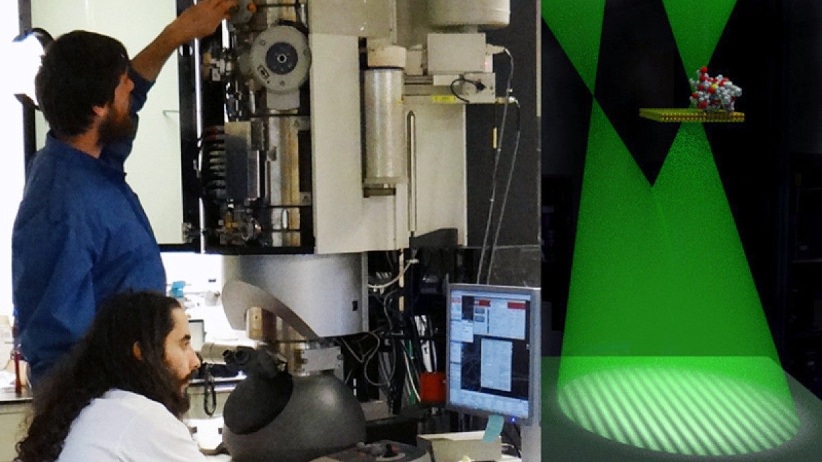
They’ve created a technique, STEM holography, that sends electrons along two separate paths, one going through a sample and one not. This allows them to measure the delay between them to create a high-resolution image. It provides improved atomic resolution of a sample’s outer structure and unveils previously unseen interfaces between a sample and underlying material.

“This technique allows us to study materials at high resolution, measure them accurately and understand them better than was possible before,” said doctoral student Fehmi Yasin. “Can we image biomolecular materials at atomic resolution without destroying them? No yet, but our technique is a good first step.”
Researchers in Germany, Japan and the United States theorized 30 years ago that such an approach was possible, but available technology did not allow them to demonstrate it as a practical imaging technique, Yasin said. UO researchers have now shown — using microscopes at the UO, Lawrence Berkeley National Laboratory and Hitachi Ltd. Research and Development Group in Japan — that STEM holography works.
The technique builds on electron holography, another recent advance that requires state-of-the-art, cost-prohibitive electron guns, specially built apertures and highly stable power supplies to deliver atomic-scale resolution.
“Using flexible STEM holography, an offshoot we developed in collaboration with Toshiaki Tanigaki at Hitachi, we now can capture with more precision the interesting geometries of materials,” Yasin said, “Previously, the field of view of STEM holography was limited to maybe 30 nanometers. Using flexible STEM holography expands the field of view.”
The first transmission electron microscope was made in Germany by Max Knoll, an electrical engineer, and Ernst Ruska, a physicist, in 1931. The first commercial version emerged in 1939. Ruska won the Nobel Prize in physics for his efforts in 1986.
The multimillion-dollar microscopes create micrographs as a beam of electrons passes through a thin slice of a sample. Traditionally in scanning transmission electron microscopes, magnetic fields are used to focus the beam to an atom-sized spot of a sample. That beam then is scanned across a sample, but large numbers of electrons are required to see anything because most of them go through a sample without getting deflected.
RELATED LINKS
The team’s four papers in 2018:
Journal of Physics D: Applied Physics:
Path-separated electron interferometry in a scanning transmission electron microscope
Nano Letters:
Probing Light Atoms at Subnanometer Resolution: Realization of Scanning Transmission Electron Microscope Holography
Applied Physics Letters:
A tunable path-separated electron interferometer with an amplitude-dividing grating beamsplitter
Physical Review Applied:
Interpretable and Efficient Interferometric Contrast in Scanning Transmission Electron Microscopy with a Diffraction-Grating Beam Splitter
The UO approach places a diffraction grating above a sample, creating additional beams hitting the sample and a hologram below it. That captures signals from electrons that are not scattered and details about how others are slowed as they pass through a sample.
The recent series of papers confirmed that STEM holography matches computer simulations.
“We put the electron microscope in conditions where we could isolate the signal that we care about, and we looked at several different kinds of samples,” said former UO doctoral student Tyler Harvey, now a postdoctoral researcher at the University of Gottingen. “We also simulated images of one sample and found that the simulations matched the experiment very well.”
In a December paper led by Harvey in the journal Physical Review Applied, the UO team detailed the technique and how it works theoretically.
In a separate paper in Nano Letters, a team led by Yasin showed that the technique provides subnanometer-resolution images of carbon-based materials. Color represents thickness, which adds a third dimension and enhances the measurements.
Images were as clear as expected with low numbers of electrons, the researchers noted.
“We think STEM holography will be a great tool for materials science and biology,” Harvey said. “The technique really excels at imaging electric and magnetic fields, and it can do that while doing the thing most materials scientists care most about: seeing where the atoms are.”
The ability to use the technique on biological specimens is a long way off, but being able to do so safely could have huge payoffs, Yasin said.
“We now have a lot of drugs that attack a cancer’s composition,” Yasin said. “But that composition is similar throughout our body, so these cancer drugs attack both diseased cells and the body’s other cells simultaneously. If we knew the position of each atom in the cancer cell, we could develop much better, more-effective drugs, without the deadly side effects.”
McMorran first wrote about the idea of using a hologram approach in a January 2011 paper in the Science, when he was with the National Institute of Standards and Technology in Maryland.
In his UO lab, supported by the National Science Foundation and U.S. Department of Energy, researchers have been pursuing four areas, all of which seek to image portions of materials that have been difficult to detect.
The four areas focus on transparent materials, including biomaterials or other organic molecules; electric fields, such as the charge and its distribution in single transistors; magnetic fields, such as materials now on hard drives and potentially useful in spintronics; and electrons and qubits expected to be used in quantum computers.
“Any four of these things might not work out,” said McMorran, who also is a member of the Materials Science Institute and Oregon Center for Optical, Molecular and Quantum Science. “There may be a better technique that ends up being best for some. We may be developing a useful tool toward getting to all four possibilities or maybe just one of them. Right now, all arrows point to all four.”
—By Jim Barlow, University Communications


